P-N Junction Diode-Diagram, Working, V-I Characteristics & Applications
Quick Exam Notes
- Definition: A P-N junction diode is made by joining p-type and n-type semiconductors.
- Working: Conducts in forward bias; blocks in reverse bias (rectification).
- Forward Bias: Current flows after threshold (0.7 V for Si, 0.3 V for Ge).
- Reverse Bias: Only small leakage current until breakdown.
- Uses: Rectifiers, clippers, clampers, signal demodulation, and switches.
Any device which allows the electric current in one direction but doesn’t allow in opposite direction is called a diode. When a semiconducting material is doped with impurity in such a way that one side has large number of acceptor impurity and other side has large number of donor impurity, we obtain a p-n junction.
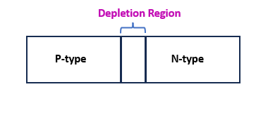
Figure 1. The diagrm of the p-n juction diode
Depletion region
When a p-n junction is formed, the p-side of the junction has a surplus of holes (positively charged carriers) and the n-side has a surplus of electrons (negatively charged carriers). These charge carriers will diffuse across the junction and recombine with each other, creating a region on either side of the junction where there is a depletion of mobile charge carriers. This region is called the depletion region.
Diffusion current
Diffusion current is the movement of charge carriers (electrons or holes) in a semiconductor due to the concentration gradient of the carriers. It is caused by the random thermal motion of the charge carriers, which causes them to move from an area of high concentration to an area of low concentration.
Drift current
Drift current is the movement of charge carriers (electrons or holes) in a semiconductor due to an applied electric field. It is caused by the acceleration of the charge carriers by the electric field, which causes them to move in a specific direction.
Lets discuss the effect when a battery is connected externally to a p-n junction diode. Depending upon the electrical connection, biasing can be of the two following types.
- Forward Bias
- Reverse bias
1. Forward bias
In forward bias, the positive terminal of the battery is connected to the p-side and the negative terminal of the battery to the n-side of the p-n junction. With the increase in bias voltage (external voltage), the width of depletion reducesand this allows more diffusion of electrons and holes which results in increase in diffusion current. However, the drift current remains almost unchanged. Hence there is a net current from p-side to n-side.
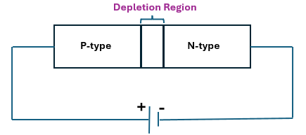
Figure 2. The forward bias of the p-n juction diode
2. Reverse bias
In reverse bias, the positive terminal of the battery is connected to the n-side and the negative terminal of the battery to the p-side of the p-n junction. With the increase in bias voltage (external voltage), the negative charge carriers (electrons) from the n-region are pulled away from the junction and positive charge carriers (holes) in the p-region are pulled away from the junction. Hence, the width of depletion increases this does not allow charge carriers to cross over the barrier allows diffusion of electrons and and thus do not contribute towards the electric current.
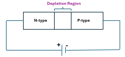
Figure 3. The reverse bias of the p-n juction diode
V-I Characteristics of p-n junction
Figure 4 shows a typical VI characteristics of a p-n junction diode under forward and reverse bias conditions. In forward bias, with increase in applied voltage, the height of potential barrier reduces to zero at a particular voltage hence there will be sharp increase in diffusion current. The voltage at which the current starts increasing rapidly is called as cut-in voltage which depends upon the material type, doping level and dopants. The junction offers a little resistance when operated in forward bias. In reverse bias, with the increase in external voltage, the barrier height increases gradually which reduces the diffusion current. Current of µA flows through the diode. Under reverse bias the junction offers high resistance.

Figure 4. V-I characteristics of p-n juction diode
For a hands-on approach to understanding the P-N junction diode experiment, visit our experiment page.
Summary
A P–N junction diode is a semiconductor device formed by joining p-type and n-type regions. It works on the principle of rectification, allowing current to flow easily in forward bias while blocking current in reverse bias. The V-I characteristics show exponential growth of current in forward bias and very small leakage current in reverse bias. This simple yet essential device is widely used in rectifiers, signal demodulation, voltage regulation, and electronic switching circuits.
MCQs on P–N Junction Diode
-
A P–N junction diode conducts current in:
- a) Both directions
- b) Forward bias only
- c) Reverse bias only
- d) Neither direction
Answer
b) Forward bias only
-
The region near the junction where carriers are depleted is called:
- a) Conduction region
- b) Valence band
- c) Depletion region
- d) Neutral region
Answer
c) Depletion region
-
The typical threshold voltage of a silicon diode is:
- a) 0.3 V
- b) 0.5 V
- c) 0.7 V
- d) 1.0 V
Answer
c) 0.7 V
-
In reverse bias, the current through a P–N junction diode is mainly due to:
- a) Majority carriers
- b) Minority carriers
- c) Drift current only
- d) Electrons only
Answer
b) Minority carriers
-
Which of the following is NOT an application of a P–N junction diode?
- a) Rectification
- b) Voltage regulation
- c) Signal demodulation
- d) Amplification
Answer
d) Amplification