Hall Effect: Theory, Definition, Formula, Derivation & Applications
Quick Exam Notes
- Definition: Hall Effect is the generation of a voltage (Hall voltage) across a semiconductor when current flows in the presence of a magnetic field.
- Formula: \( R_H = \frac{V_H \times w}{I \times B} \)
- Hall Coefficient: \( R_H = \frac{1}{nq} \), helps identify charge carrier type.
- Applications: Used in Hall sensors, magnetic field measurement, and semiconductor characterization.
- Key Point: Positive \( R_H \rightarrow \) p-type; Negative \( R_H \rightarrow \) n-type semiconductor.
- Scroll to the end of the page to explore the Interactive Visualization demo of Hall effect.
Principle
When a current carrying semiconductor is placed in a transverse magnetic field, a voltage is induced in the semiconductor direction perpendicular to both the current and magnetic field. This phenomenon is called Hall effect. The induced voltage is called Hall voltage (VH). It was discovered by Hall in 1879.
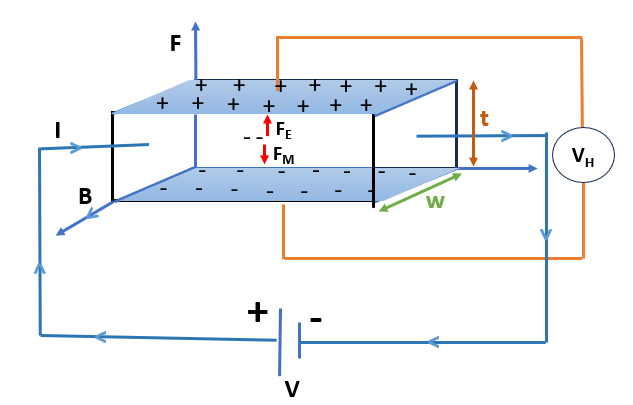
Figure 1. Schematic diagram of the Hall effect experiment.
Theory
Consider a rectangular slab of an n-type semiconductor material of width (w), thickness (t) and that carries a current I along the positive X-direction and magnetic field B be applied along the positive Z-direction. Under the influence of this magnetic field, the electron experience a force called Lorentz force given by
\[ \vec{F}_M = q (\vec{v}_d \times \vec{B}_z) \tag{1} \]This Lorentz force is exerted on the electrons in the negative Y-direction. The direction of this force is given by Fleming’s left-hand rule. Thus, the electrons are, therefore, deflected downwards and collect at the bottom surface of the specimen.
\[ \vec{F}_M = -e (\vec{v}_d \times \vec{B}_z) \]
\[ \vec{F}_M = -e (\vec{v}_d \vec{B}_z) \sin 90^\circ \]
\[ \vec{F}_M = -e \vec{v}_d \vec{B}_z \tag{2} \]
On the other hand, the top edge of the specimen becomes positively charged due to the loss of electrons. Hence, a potential called the Hall voltage VH is developed between the upper and lower surfaces of the specimen, which establishes an electric field E called the Hallfield across the specimen in the negative Y-direction
The force acts on the charges in the presence of generated electric field,
\[ \vec{F}_E = -e \vec{E}_H \tag{3} \]Under the equilibrium condition, the force due to electric component will counter balance that of magnetic force.
\[ F_E = F_M \] \[ v_d = \frac{E_H}{B_z} \tag{4} \]The current density the semiconductor will be,
\[ J_x = -ne v_d \tag{5} \]Substitute vd value in Eqn 5,
\[ J_x = \frac{-ne E_H}{B_z} \tag{9} \]Where \( R_H = - 1/ne \) is the Hall co-efficient.
We can write \( R_H \) as
\[ R_H = \frac{E_H}{J_x B_z} = \frac{V_H}{t J_x B_z} \tag{11} \]where \( E_H = \frac{V_H}{t} \)
We know current density \( J_x = \frac{I}{A} = \frac{I}{(w \times t)} \). Hence \( R_H \) will be
\[ R_H = \frac{V_H \times w \times t}{t \times B_z \times I} \tag{12} \] \[ R_H = \frac{V_H \times w}{I \times B_z} \tag{13} \]If \( R_H \) is positive, it is a p-type semiconductor. If \( R_H \) is negative, it is an n-type semiconductor.
Applications of Hall effect
- To asses the type of semiconductor, whether it is a p-type or n-type.
- The evaluation of concentration of charge carriers.
- The calculation of mobility of charge carriers.
\[ \sigma = n e \mu; \mu = \sigma R_H \]
- To measure the strength and direction of magnetic field.
Summary
The Hall Effect is a powerful tool in semiconductor physics, allowing us to identify the type of charge carriers and calculate their density. By applying a magnetic field perpendicular to a conductor or semiconductor carrying current, a transverse voltage known as Hall voltage is produced. This effect is widely used to determine carrier mobility, concentration, and to design sensors in practical electronics. Solving numerical problems on the Hall Effect strengthens conceptual understanding and prepares students for engineering and physics exams.
MCQs on Hall Effect
-
The Hall Effect occurs when:
- a) A conductor is heated
- b) A current-carrying conductor is placed in a magnetic field
- c) Light falls on a semiconductor
- d) A conductor is cooled
Answer
b) A current-carrying conductor is placed in a magnetic field
-
The Hall Coefficient \( R_H \) is given by:
- a) \( R_H = \frac{1}{nq} \)
- b) \( R_H = nq \)
- c) \( R_H = \frac{V}{IR} \)
- d) \( R_H = \frac{I}{Vq} \)
Answer
a) \( R_H = \frac{1}{nq} \)
-
A positive Hall Coefficient indicates:
- a) n-type semiconductor
- b) p-type semiconductor
- c) Insulator
- d) Metal
Answer
b) p-type semiconductor
-
The Hall voltage depends on:
- a) Current, magnetic field, and sample thickness
- b) Temperature only
- c) Only current
- d) Resistance of the material
Answer
a) Current, magnetic field, and sample thickness
-
The Hall Effect is widely used to:
- a) Measure resistance
- b) Measure magnetic field and identify charge carriers
- c) Generate electricity
- d) Store energy
Answer
b) Measure magnetic field and identify charge carriers
Related Topics
Interested in performing the Hall Effect experiment yourself? Explore the lab procedure and setup.