P-N Junction Diode
Aim
To study the voltage-current (V-I) characteristics of a p-n junction diode under forward bias and reverse bias conditions and analyze its behavior as a semiconductor device.
Apparatus
- p-n junction diode (e.g., 1N4007)
- DC power supply (0-30V)
- Resistor (e.g., 1 kΩ)
- Milli and Micro Ammeter
- Connecting wires
- Breadboard
- Voltmeter
Pre-Lab Questions
- What is a p-n junction diode?
A p-n junction diode is a semiconductor device formed by joining p-type and n-type materials, allowing current to flow in one direction only when forward-biased. - What is forward bias in a diode?
Forward bias occurs when the p-side is connected to the positive terminal and the n-side to the negative terminal of a power supply, reducing the barrier potential and allowing current to flow. - What is reverse bias in a diode?
Reverse bias occurs when the p-side is connected to the negative terminal and the n-side to the positive terminal, increasing the barrier potential and preventing significant current flow. - What is the significance of the knee voltage in forward bias?
The knee voltage (or threshold voltage) is the minimum voltage required to overcome the depletion region barrier and allow significant current to flow (e.g., ~0.7V for silicon diodes). - What is the need for doping in intrinsic semiconductor?
Doping an intrinsic semiconductor introduces impurities to increase its conductivity by adding charge carriers (electrons or holes). This transforms it into an extrinsic semiconductor, enabling practical use in devices like diodes and transistors - How depletion region is formed in the p-n junction?
The depletion region forms at the P-N junction when electrons from the N-type material diffuse into the P-type material and recombine with holes, creating a zone of immobile charged ions that blocks further charge movement. This process establishes a potential barrier, depleting the area of free charge carriers. - What happens to a diode in reverse bias beyond its breakdown voltage?
Beyond the breakdown voltage, the diode conducts heavily due to avalanche or Zener effect, which may damage it unless it’s a Zener diode designed for this purpose. - Define diode resistance
Diode resistance refers to how much a diode resists current flow, defined as the ratio of voltage across it to the current through it.
Theory
- Forward Bias: When the p-side is positive relative to the n-side, the depletion region narrows, and beyond the knee voltage (e.g., 0.7V for silicon), current increases exponentially due to the movement of majority carriers.
- Reverse Bias: When the p-side is negative relative to the n-side, the depletion region widens, and only a small leakage current (due to minority carriers) flows until the breakdown voltage is reached. The V-I characteristics are non-linear, showing diode rectification properties.
Need a refresher on the concepts? Check out our detailed explanation of the P-N junction theory
Circuit Diagram
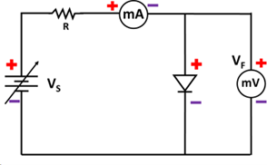
Circuit diagram for forward bias

Circuit diagram for reverse bias
Procedure
- Forward Bias Setup:
- Connect the diode in forward bias (anode to positive, cathode to negative) with a 1 kΩ resistor in series on a breadboard.
- Use a multimeter in parallel to measure VD and in series to measure I.
- Increase the supply voltage from 0V in steps of 0.1V up to 1V, then in steps of 0.5V up to 5V.
- Record \(V_F\) and \(I\) for each step.
- Plot V-I characteristics graph for forward bias taking voltage along X-axis and current along Y-axis.
- Reverse Bias Setup:
- Reverse the diode connections (anode to negative, cathode to positive).
- Increase the supply voltage from 0V in steps of 1V up to 10V (avoid exceeding breakdown voltage).
- Record \(V_R\) and \(I\) for each step.
- Plot V-I characteristics graph for reverse bias taking voltage along X-axis and current along Y-axis.
Observation Table
Forward Bias
| \(V_S (V)\) | \(I_F (mA)\) | \(V_F (V)\) |
|---|---|---|
| 1 | ||
| 2 | ||
| 3 | ||
| 4 | ||
| 5 | ||
| . | ||
| . | ||
| 15 |
Reverse Bias
| \(V_S (V)\) | \(I_R ( \mu A)\) | \(V_R (V)\) |
|---|---|---|
| 1 | ||
| 2 | ||
| 3 | ||
| 4 | ||
| 5 | ||
| . | ||
| . | ||
| 15 |
Calculations
- Knee Voltage (Vk): From the forward bias table, identify the voltage where current increases significantly (e.g., 0.7V).
- Dynamic forward resistance::
\[ \Delta R_F = \frac{\Delta V_F}{\Delta I_F} \]
Example:
\[ \Delta R_F = \frac{5-4}{(4-2)\times 10^{-3}} =0.5\times 10^{3} = \color{red}{0.5 kHz} \] - Dynamic forward resistance::
\[ \Delta R_R = \frac{\Delta V_R}{\Delta I_R} \]Example:
\[ \Delta R_F = \frac{5-4}{(4-2)\times 10^{-6}} =0.5\times 10^{6} = \color{red}{0.5 MHz} \]
Model Graph

V-I Characteristics of P-N junction diode under forward & reverse bias
Precautions
- Do not exceed the maximum current rating of the LED (typically 20-30 mA).
- Ensure correct polarity of the LED (anode to positive, cathode to negative).
- Use a suitable resistor to limit current.
- Take readings carefully to avoid parallax error in the multimeter.
- Avoid prolonged high voltage to prevent LED burnout.
Applications
- Rectifiers in power supplies (AC to DC conversion).
- Signal demodulation in communication circuits.
- Voltage regulation (e.g., Zener diodes).
- Protection circuits in electronics.
- Switching applications in digital circuits.
Post-Lab Questions
- What did you observe about the current in forward bias below the knee voltage?
The current was negligible until the knee voltage was reached. - What is cut-in or knee voltage? Specify its value in case of Ge or Si?
Cut-in voltage (also called knee voltage) is the minimum voltage required for a PN junction diode to start conducting significantly in the forward-biased condition. Below this voltage, the current is very small, and beyond this point, the current increases rapidly.
Si: 0.7 V
Ge: 0.3 V - Why does the current increase exponentially in forward bias?
Beyond the knee voltage, the depletion region barrier is overcome, allowing majority carriers to flow freely, resulting in exponential current rise. - Why is the reverse bias current so small?
In reverse bias, the depletion region widens, and only minority carriers contribute to a small leakage current. - How does P-N junction diode act as a switch?
In forward bias, a P-N junction diode conducts current like a closed switch by reducing the depletion region. In reverse bias, it blocks current like an open switch by widening the depletion region. - What is the practical significance of the diode’s rectification property?
It allows diodes to convert AC to DC, essential for power supplies. - What would happen if the reverse voltage exceeded the breakdown voltage?
The diode would conduct heavily, potentially getting damaged unless designed as a Zener diode. - What is the effect of forward and reverse biases on the width of depletion region in P-N junction diode?
In forward bias, the depletion region width decreases as the applied voltage reduces the barrier, allowing current to flow. In reverse bias, the depletion region width increases as the voltage strengthens the barrier, blocking current.
Outcomes
- Successfully studied the V-I characteristics of a p-n junction diode under forward and reverse bias.
- Determined the knee voltage in forward bias (e.g., ~0.7V for Silicon).
- Confirmed the diode’s rectification behavior: conducting in forward bias and blocking in reverse bias.