Transmission Electron Microscope (TEM)
Transmission Electron Microscope (TEM) is an advanced electron microscopy technique that uses a high-energy electron beam transmitted through an ultra-thin specimen to obtain high-resolution images of the internal structure, crystal lattice, and defects of materials at atomic and nanometer scales.
Introduction
The Transmission Electron Microscope (TEM) is one of the most powerful characterization tools in nanotechnology, materials science, and solid-state physics. Unlike SEM, which provides surface information, TEM reveals the internal structure of materials by allowing electrons to pass through thin specimens. TEM offers extremely high resolution, often down to the atomic scale.
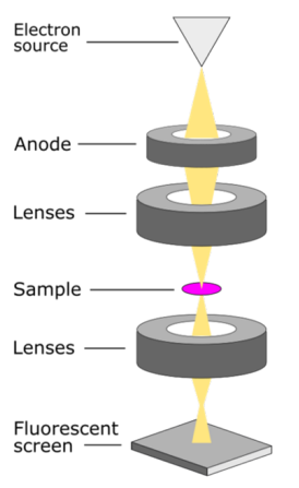
Figure 2. Interaction of transmitted electrons with thin specimen
Main Components of TEM
- Electron gun (thermionic or field emission source)
- Condenser lens system
- Ultra-thin specimen holder
- Objective, intermediate, and projector lenses
- Fluorescent screen or digital camera
- High-vacuum system
Principle and Working of Transmission Electron Microscope
- The principle of TEM is based on the transmission of a highly focused electron beam through a very thin specimen (typically less than 100 nm thick).
- When electrons interact with the atoms inside the specimen, they undergo scattering, diffraction, and phase changes depending on the internal structure.
- The transmitted and diffracted electrons carry information about the crystal structure, defects, grain boundaries, and atomic arrangement.
- Electromagnetic lenses magnify the transmitted electron image, which is projected onto a fluorescent screen or recorded by a camera.
- Diffraction patterns obtained in TEM provide crystallographic information such as lattice spacing and crystal orientation.
- Thus, TEM enables direct visualization of internal structures with atomic-scale resolution.
Applications of TEM
- Atomic-scale imaging of nanomaterials
- Crystal structure and lattice defect analysis
- Phase identification using electron diffraction
- Study of nanoparticles, nanotubes, and thin films
- Biological imaging of viruses and cell organelles
Advantages of TEM
- Extremely high resolution (up to atomic scale)
- Provides detailed internal structural information
- Simultaneous imaging and diffraction analysis
- Essential for nanoscience and crystallography
Limitations of TEM
- Requires ultra-thin specimen preparation
- Complex and time-consuming sample preparation
- High cost of instrument and maintenance
- Electron beam damage to sensitive materials
Related topics: Synthesis of Nanomaterials | Sol-Gel Method | Ball Milling Method